Introduction
Sometimes it's desirable to specify a region where no isolation routing should be done, or perhaps perform copper clearing only within a certain polygon.
In this tutorial:
- Selective Isolation Routing - Example 1
- Selective Isolation Routing - Example 2
- Selective Copper Clearing - Example
Selective Isolation Routing - Example 1
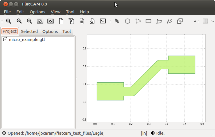
We shall start by loading the Gerber file describing out circuit board:
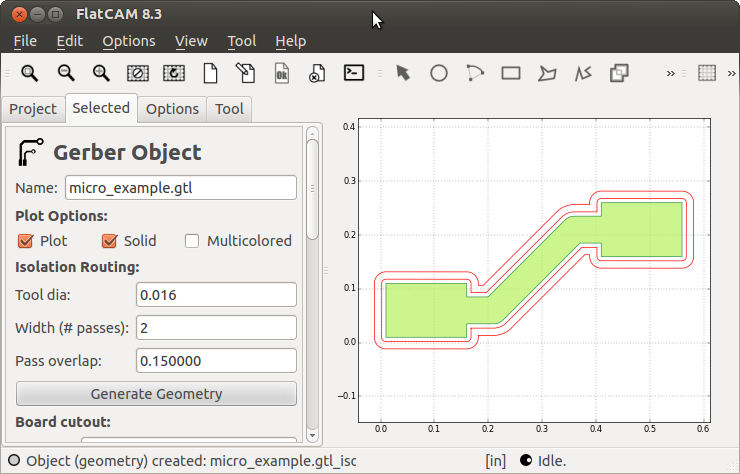
And we shall create a 2-pass isolation routing geometry:
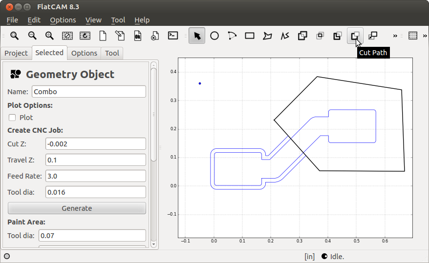
In our example, we want to specify an area where no isolation routing is allowed. In the figure below, we have started the drawing tool and drawn a polygon for this "forbidden" area.
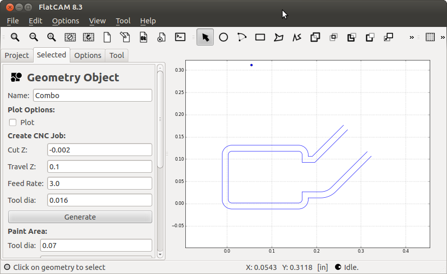
We have carried out a few steps to get here: The isolation routing operation from before created 2 geometry objects. We have joined them using Edit→Join Geometry and deleted the original 2 objects. Then we've hidden the plots for the Gerber and the "Combo" geometry.
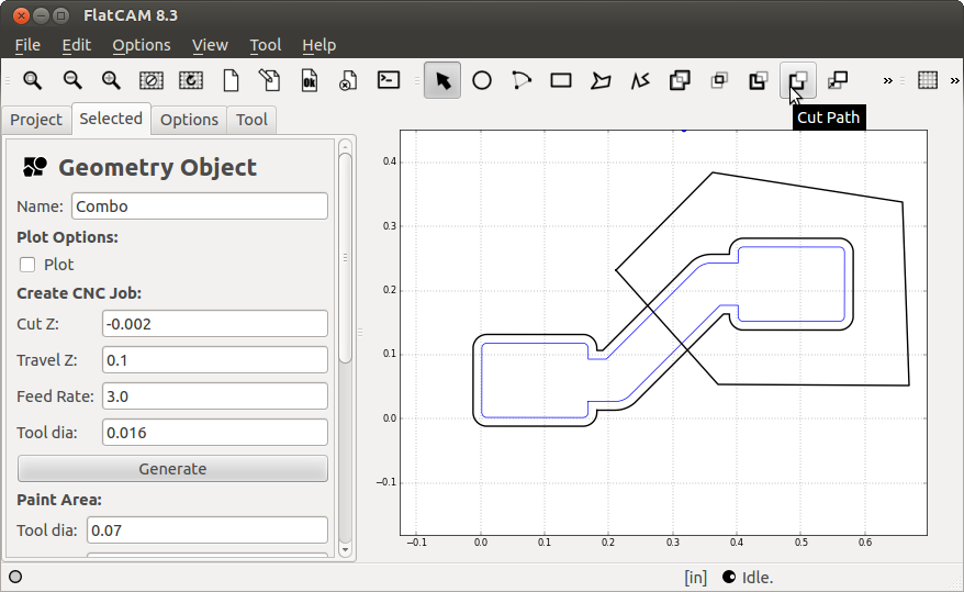
We want to select the isolation path to be the "target" and the forbidden polygon to be the "tool" for the Cut Path operation. For this, you just have to select them in that order. Then click on the Cut Path button. The result is shown below.
Just repeat for the second path to get the final result.